
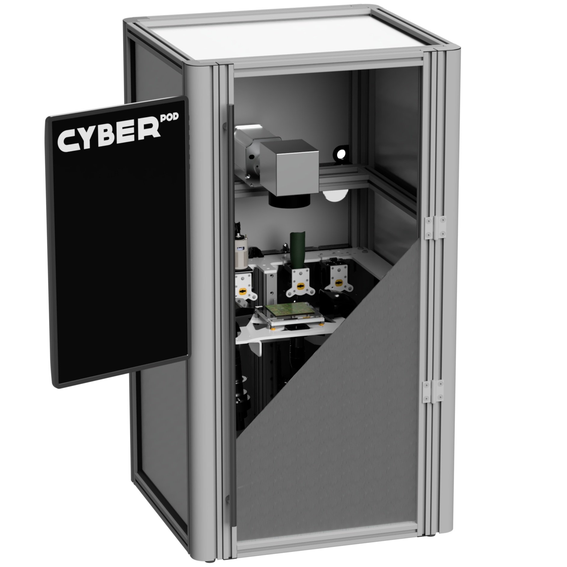

PCB Prototyping System
For 70 years, prototyping of PCBs has relied on large factories, fixed tooling, order pooling to cut costs, and extensive manual labor to build prototypes with equipment optimized for mass manufacturing.
To accelerate innovation in the industry, Cyber POD built its PCB Prototyping System, an autonomous machine optimized for rapid prototyping.
Up to 8 Layer PCBs.
Up to 100 mm x 100 mm Size.
Fabrication Time from 2 to 8 Hours.

Our technology was developed specifically for cell-based fabrication instead of the traditional photolithography production line. Therefore It is optimized for rapid prototyping and small to medium volume production of mass customized smart products.
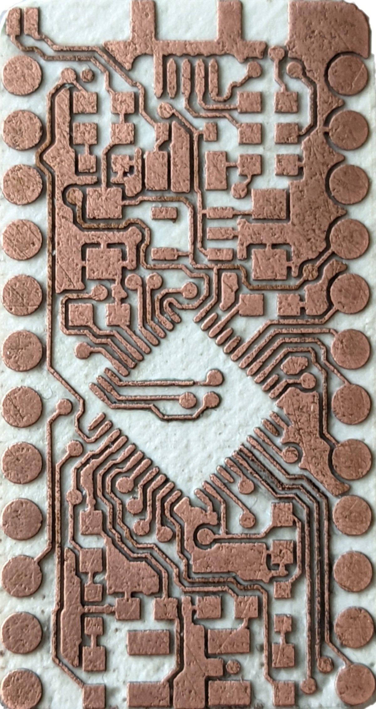
~20% of Bulk Copper Conductivity
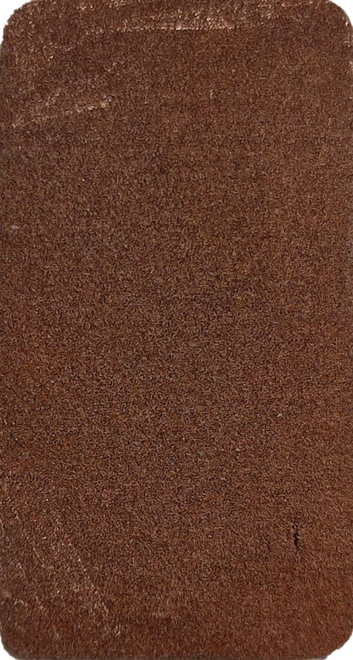
Glass Fiber Reinforced High-Temp. Dielectric Material
Minimal Copper Layer Thickness - 35μm
Resolution: Minimal Trace Width/Space - 150μm

FDM 3D Printing of Dielectric Material

FDM 3D Printing of Conductive Material
Thermal Debinding and Laser Sintering
Laser Structuring
Dielectric Material Overprinting and Surface Facing